

It is hard to overstate how much of our modern existence rests on a device that started as a simple audio tool. Before the mid-20th century, electronics were heavy, hot, and unreliable. The public depended on vacuum tubes for everything from radios to early computers. They were fragile. They burned out frequently. They generated enough heat to warp equipment. Then came the transistor.
Developed in 1947 by engineers at Bell Laboratories, the original goal was modest. They needed a way to amplify sound over telephone lines. The vacuum tube was the standard, but it was clumsy. The new device replaced it with something solid-state. It was smaller. It was cooler. It was more reliable.
The first iteration was a point-contact transistor. It measured half an inch tall. Roughly 1.27 centimeters. It wasn’t particularly powerful by today’s standards, but physicists saw the potential immediately. Engineers began slotting these tiny switches into radios and other electronics. They learned to shrink them. They learned to make them more efficient.
This relentless miniaturization led to a major leap in 1958. Engineers attached two transistors to a single silicon crystal. They created the first integrated circuit. This was the bridge to the microprocessor. If a computer is a body, the microprocessor is the brain. It processes data. It makes calculations. Without the integrated circuit, that brain never forms.
Moore’s Law and the Silicon Crunch
By the 1960s, the pace of innovation had a name. Gordon Moore, a computer scientist and co-founder of Intel, noticed a pattern. He observed that engineers were doubling the number of transistors on a square inch of silicon every twelve months. It happened like clockwork. Size went down. Density went up.
This trend gave us the personal computer. The smartphone. The MP3 player. Without these tiny switches, we would still be clicking mechanical switches and relying on vacuum tubes to perform basic math. The shrinking trend continued for decades. But it hasn’t quite kept up with Moore’s original prediction. Today, the doubling cycle takes about 24 months. It is slower. But the result is the same. We pack more power into smaller spaces.
So, how small can a transistor get? In 1947, that first device was over one-hundredth of a meter high. By the 2010s, Intel was producing microprocessors with transistors just 45 nanometers wide. A nanometer is one-billionth of a meter. The scale is difficult to comprehend.
Physical Limits and Future Chips
Manufacturers are already working on the next generation. Chips are moving toward transistors that are only 32 nanometers wide. But some physicists and engineers are sounding the alarm. We might be bumping into fundamental physical limits. Quantum effects start to interfere when things get this small. Electrons tunnel through barriers they shouldn’t. Heat becomes a nightmare.
The history of the transistor is not just about engineering. It is about our relentless drive to make things smaller. Faster. More efficient. We hit a wall. The wall is physical law. But we keep pushing. The next few years will tell us if we break through or if we’ve reached the end of the line for silicon.
Anatomy of a Transistor
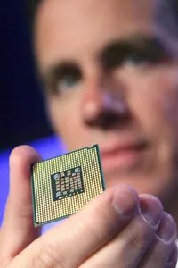
To understand why computers are hitting a wall, you first have to understand what a transistor is. It isn’t magic. It’s a switch. And not just any switch. It’s a switch built from matter that behaves strangely under pressure.
Matter generally falls into three buckets.
Conductors let electricity flow freely. Think copper. It has plenty of free electrons ready to move.
Insulators block flow completely. Glass. Ceramic. The electrons are stuck.
Then there are the semiconductors. Silicon sits in the middle. It has some electron space, but not enough to conduct like a metal. It’s stubborn. It needs a nudge.
That nudge is the key. By tweaking conditions, engineers force silicon to toggle between conducting and insulating. This binary behavior—on and off—is the bedrock of all modern computing. But getting silicon to behave requires a process called doping.
Doping and the Substrate
Engineers introduce specific impurities into silicon to change its electrical properties. They start with a base material called a substrate.
In our example, we are looking at an n-type transistor. This means the substrate is positively charged.
To make this work, you need three specific terminals on top of that substrate:
- Source
- Drain
- Gate
The gate sits between the source and the drain. It acts as a one-way valve for voltage. It lets electricity push into the silicon, but the design prevents it from flowing back out.
How? The gate is separated from the substrate by a thin oxide layer. This insulator stops electrons from crossing directly through the gate terminal.
In an n-type transistor, the source and drain are negatively charged. When you apply a positive voltage to the gate, something physical happens inside the silicon.
The Electron Channel
Apply positive voltage to the gate.
This attracts the free electrons in the positively charged substrate. They pile up against the oxide layer under the gate.
This creates an electron channel.
A bridge of conductivity forms between the source and the drain.
If you then push a positive voltage into the drain, electrons flow. They travel from the source, through that newly formed channel, and out to the drain.
Remove the voltage from the gate? The attraction vanishes. The electrons scatter. The channel collapses.
Current stops.
This is how a transistor acts as a switch.
- Voltage on gate = On
- No voltage on gate = Off
Computers read this binary state as bits. One. Zero. One. Zero. Your entire digital life is built on billions of these tiny, physical switches flipping back and forth.
P-Type Variations
We used an n-type transistor for clarity. But p-type transistors exist too.
In a p-type setup, you reverse the charges. The substrate is doped with negatively charged material. The terminals carry a positive charge. The logic remains the same, but the physics of the charge carriers flip.
Most modern chips use a combination of both types, known as CMOS technology, to minimize power consumption. But before we get to the architecture, we have to face the hardware.
Transistors on the Nanoscale
The problem isn’t the concept. The concept works. The problem is size.
As transistors shrink to fit more of them onto a chip, quantum effects start to bleed in. Electrons tunnel through barriers they shouldn’t be able to cross. The oxide layer gets so thin that electrons leak through it even when the gate is off.
This leakage kills battery life. It generates heat. And it creates errors.
We’ve been miniaturizing transistors for decades. We’re running out of room to squeeze them smaller without breaking the laws of physics.
What happens when the switch itself becomes unreliable?
Why Transistor Shrinkage Is Hitting a Physical Wall
Journalists love to predict the death of Moore’s Law. Every year, someone publishes a piece declaring that transistors have hit their size limit. Then engineers find a workaround. The transistor gets smaller. The prediction is wrong. We are in a cycle of false alarms, partly because writers have become gun-shy about calling the endgame.
But the endgame is real. It is not a matter of engineering skill. It is a matter of physics.
Once you hit the nanoscale, you leave behind classic physics. You enter the world of quantum mechanics. Here, matter and energy act on rules that seem counterintuitive. You cannot even observe a quantum system without changing its behavior.
If electrons can pass through a gate under any set of circumstances, there is no way to control their flow.
The biggest problem is electron tunneling. Think of it as teleportation. When a material barrier is extremely thin—about one nanometer, or the width of ten atoms—electrons can pass right through it. They do not make a hole. They do not punch through. The electron simply disappears on one side and reappears on the other.
Gates are supposed to control electron flow. If electrons tunnel through the gate, the control is lost. You get leaky transistors. The processor becomes ineffective. It might not even function.
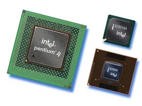
Companies like Intel are already working with transistors around 32 nanometers wide. The oxide layer is getting dangerously thin. In the past, engineers have always found a way around these obstacles. They keep up with Moore’s Law. But this time, they are facing a fundamental law of nature.
Engineers might find an effective insulator at one nanometer. It is possible. But even then, there is not much further to go with traditional transistors. Beyond the nanoscale is the atomic scale. Here, materials are only a few atoms in size. You run out of material to work with.
This does not mean transistors will vanish. It means the exponential growth in microprocessor development will slow down. It will level off. Improvements in raw processing power will not continue at the same breakneck pace.
But manufacturers will still find ways to improve efficiency. Performance will increase, just not exponentially.
There is another possibility. Microprocessor makers are looking for alternatives to traditional transistors. Some are already trying to harness quantum effects at the nanoscale. They are turning nano-lemons into nano-lemonade.
Moore’s Law might only last a few more years. But if you look back decades, journalists made the same claim. Engineers likely see these predictions as a personal challenge. They will keep pushing. But the laws of physics are a hard wall to break.
Small Packages
The Intel Atom is a collection of small but mighty processors designed to work on smartphones.